SIDDHARTA-2 — The apparatus
2. The Silicon Drift Detectors
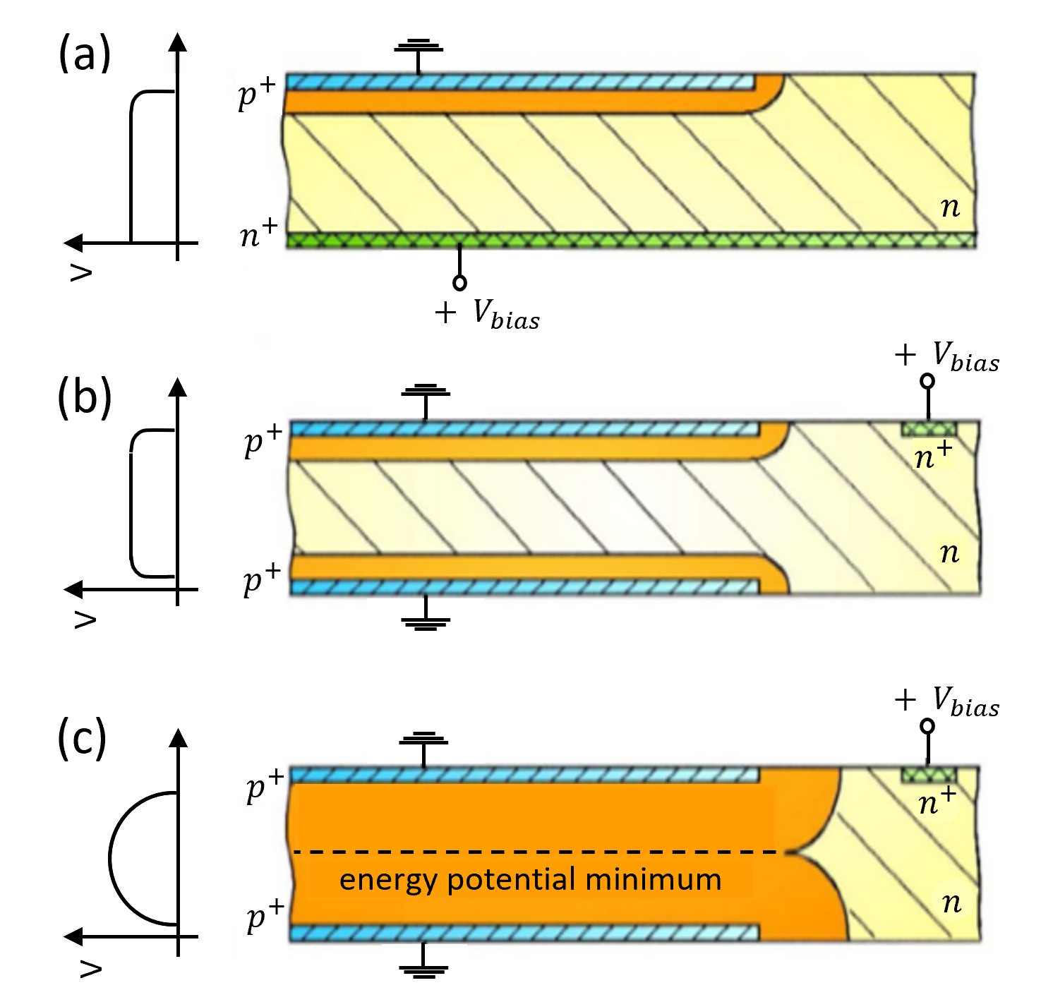
Silicon Drift Detectors (SDDs) are semiconductor detectors proposed for the first time in 1983 by Paul Rehak and Emanuele Gatti [1,2]. Semiconductor detectors measure the energy of the crossing particles by the collection of the electron-hole pairs produced in the sensitive volume of the detector. The working principle of an SDD is based on the creation of a large lateral depleted zone of a p − n junction within the silicon bulk, obtained by biasing a small n+ anode with higher voltage concerning the two p+ electrodes laying on both surfaces of an n-type silicon bulk. A reverse polarization is applied to enlarge the depletion zone and to separate the electron-hole pairs. With a sufficiently high biasing voltage, both the depletion regions, separated in equilibrium conditions, join together, drastically increasing the sensitive volume of the SDD detector. A small non-depleted region is located near the n+ electrode. This operating procedure allows reaching large depletion zones by applying a bias voltage four times less than the usual ones (g.e. around 350 μm of thickness applying around 100 V) [2,3].
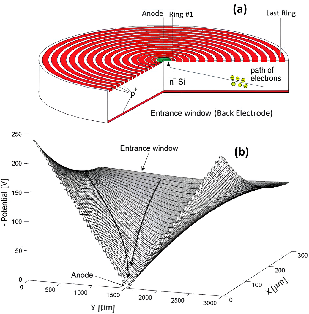
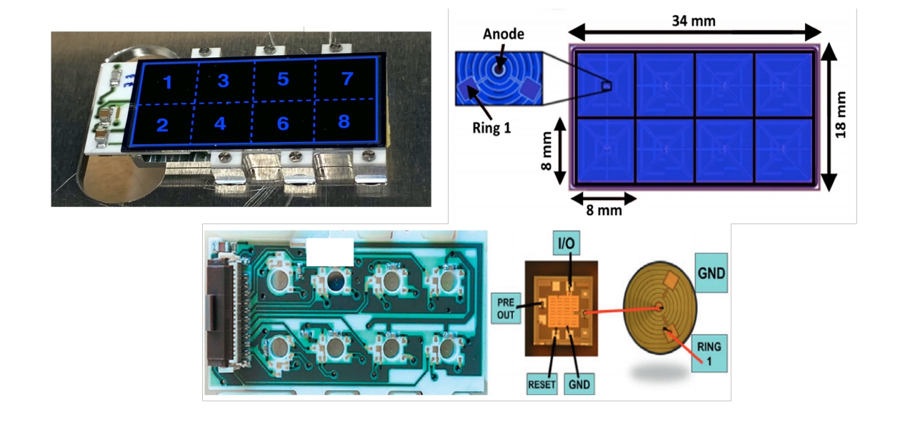
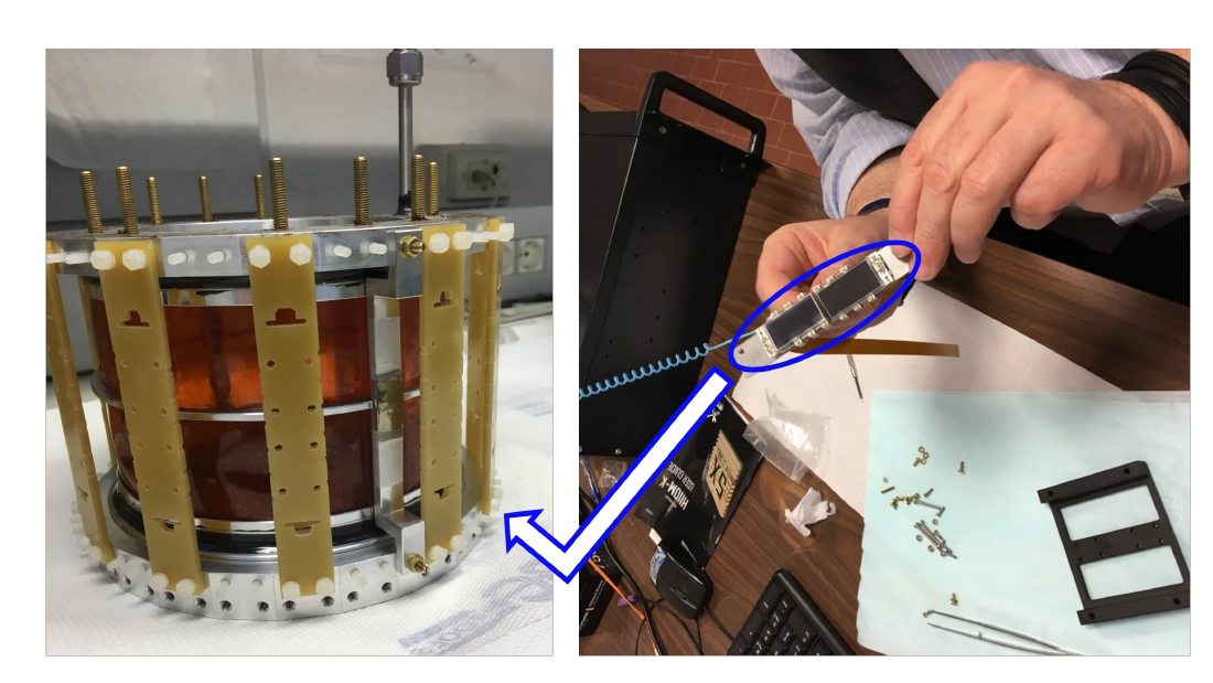
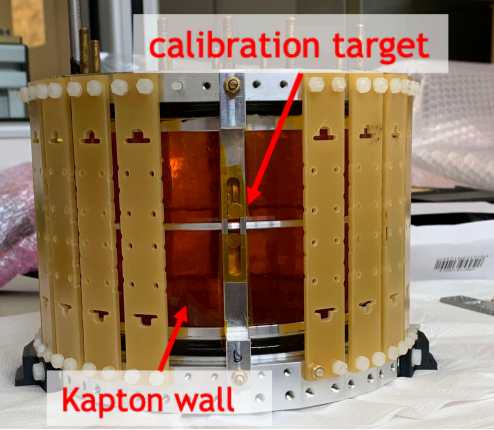
The SDDs installed in the SIDDHARTA-2 experiment have a thickness of 450 μm and allow the x-ray detection in the 4-40 keV energy range with high efficiency [5,6]. The SDDs are organized in 2 × 4 matrices of 5.12 cm2 each, with a 75% active area. The SIDDHARTA-2 experiment has 384 SDDs radially surrounding the cylindrical shape of the cryogenic target. The SDDs are cooled down to a temperature of about 120 K with a cryo-cooler circuit [7]. A low-noise charge sensitive preamplifier (CUBE) [8], represents the first stage of the signal processing, together with the front-end readout based on the SFERA ASIC [9,10] and includes fast and slow shapers with programmable parameters in order to improve the spectroscopic response of the system. Each SFERA chip, after processing the signals coming from two SDDs arrays, provides the charge and the timing information of the detected event to the downstream data acquisition system. The timing measurement in particular is essential to suppress the asynchronous background which originates from the accelerator [11]. The target and the SDDs are placed inside a vacuum chamber and kept at a pressure below 10-5 mbar. These pressure and temperature conditions allow high-quality performances of the SDDs, which provide a resolution of 160 eV and a detection efficiency of almost 100% at 6 keV, the energy value close which the kaonic deuterium 2p→1s transition is expected [12]. The SDDs’ energy calibration is performed with x-ray tubes emitting through high purity titanium and copper strips placed on the target cell walls. The calibration method is described in [7] and in the dedicated page.
References
-
-
[1]. E. Gatti and P. Rehak, Semiconductor drift chamber — An application of a novel charge transport scheme, Nucl. Instr. Meth. Phys. Res. 225, 608 (1984).
-
[2]. E. Gatti and P. Rehak, Semiconductor drift chambers for position and energy measurements, Nucl. Instr. Meth. Phys. Res. Sect. A 235, 224 (1985).
-
[3]. E. Gatti and P. Rehak, Progress in semiconductor drift detectors, Nucl. Instr. Meth. Phys. Res. Sect. A 248, 367 (1986).
-
[4]. E. Gatti and P. Rehak, Electron injection in semiconductor drift chambers, Nucl. Instr. Meth. Phys. Res. Sect. A 295, 489 (1990).
-
[5]. M. Miliucci et al., Silicon drift detectors technology for high precision light Kaonic atoms spectroscopic measurements at the DAΦNE collider, AIP Conference Proceedings 2416, 020009 (2021).
-
[6]. A. D. Butt et al., Characterization of monolithic SDD arrays and SFERA ASIC for the SIDDHARTA experiment, IEEE Nuclear Science Symposium, Medical Imaging Conference and Room-Temperature Semiconductor Detector Workshop (NSS/MIC/RTSD) 1-4 (2016).
-
[7]. F. Sgaramella et al., The SIDDHARTA-2 calibration method for high precision kaonic atoms x-ray spectroscopy measurements, Physica Scripta 97, 11 (2022).
-
[8]. L. Bombelli et al., “CUBE”, A low-noise CMOS preamplifier as alternative to JFET front-end for high-count rate spectroscopy, 2011 IEEE Nuclear Science Symposium Conference Record, 1972-1975 (2011).
-
[9]. F. Schembari et al., SFERA: An Integrated Circuit for the Readout of X and γ -Ray Detectors, IEEE Trans. Nucl. Sci. 63, 1797 (2016).
-
[10]. R. Quaglia et al., Development of arrays of Silicon Drift Detectors and readout ASIC for the SIDDHARTA experiment, Nucl. Instrum. Meth. A 824, 449 (2016).
-
[11]. L. De Paolis et al., Trigger rejection factor in the first kaonic helium run with the complete SIDDHARTA-2 setup, EPJ Web of Conferences 270, 00028 (2022).
-
[12]. M. Miliucci et al., Silicon drift detectors system for high-precision light kaonic atoms spectroscopy, Meas. Sci. Technol. 32 095501 32, 095501 (2021).
-